Introduction
In an earlier post I looked at coaxial cables over a ground plane as multiconductor transmission lines. This was to understand quarter wave folded balun operation. Computing the transmission line inductances, however, I realized that the current distribution would depend on how the return current flows.If the current flows through the center conductor and returns through the shield, the current would be most concentrated on the outside of the center conductor, and return current would concentrate on the inside of the shield. However, if the current flows through the shield and returns through a the ground plane, then the current in the shield would concentrate on the outside part of the shield facing toward the ground plane - and return current would concentrate on the ground plane surface closest to the cable. This concentration of the current is caused by what is known as the skin and proximity effects.
The figures below show a visualization of the current density in a coax under the previously descibed situations. Coax geometry is that of RG316, which is placed very close to a ground plane. The right hand side figure shows the situation where current flows through the inner and back through the shield. while the left hand side shows the situation where current flows through the shield and back through the ground plane. Color indicates current density: dark red is maximal density into the display, dark blue is maximal density out of the display and light green is zero current density. The current is driven by a sinusoidally oscillating uniform electromotive force.


All computations in this article are performed using scikit-fem and my own code, and visualized using matplotlib.
The calculations in my earlier post didn't take these effects into account, and the current assumed a uniform density in the entire conductor in each case. This caused the inductance matrix of the transmission line system to be somewhat incorrect. I mentioned it at the time of writing that post, that accounting for this would be a whole new can of worms. It's now time to open that can.
Deriving the appropriate equations
I'll try to keep the following fairly general, but here we are mostly interested in a long multiconductor transmission line (with n conductors), with dielectrics separating the conductors from each other. The cross-section of the transmission line is assumed to remain constant along its length.
To simplify notation, we'll consider all fields as time-harmonic at frequency w, such that e.g. \(\mathbf{B}(x,y,z,t) = \mathrm{Re} \{ \mathbf{B}(x,y,z) \exp(i \omega t) \}\), and omit the time variable in the following. In particular, we'll omit writing down the time derivative operators and just expand out the result.
Let's start with Ampere-Maxwell's law
\[\nabla \times \mathbf{H} = \mathbf{J} + i\omega \mathbf{D}\]
Inside the conductors we assume Drude's conduction model. The model gives us that \(\mathbf{J} = \sigma \mathbf{E}\) (when considering time scales significantly longer than the mean collision time). Also, it states that there is no polarization in the medium, giving \(\mathbf{D} = \epsilon_0 \mathbf{E}\). (Note: alternatively we could have assumed that there is no conduction current \(\mathbf{J}\), but that we're dealing with an extremely lossy dielectric medium. This would have been represented by a large imaginary component of the permittivity).
Following Drude, inside the conductor we have
\[\nabla \times \mathbf{H} = \sigma \mathbf{E} + i\omega \epsilon_0 \mathbf{E}\]
However, for copper and the frequencies we're intersted in, \(\sigma \mathbf{E}\) dominates \(i\omega \epsilon_0 \mathbf{E}\) by more than a factor of a million, so we'll ignore the term \(i\omega \epsilon_0 \mathbf{E}\).
Inside the insulators we assume no conduction and that \(\mathbf{D} = \epsilon \mathbf{E}\), where \(\epsilon\) is the permittivity of the insulator (and is taken as different within each material). This gives
\[\nabla \times \mathbf{H} = i\omega \epsilon \mathbf{E}\]
Again, for the materials and frequencies we're interested in, \(i\omega \epsilon \mathbf{E}\) significantly smaller than \(\sigma \mathbf{E}\), and thus we can ignore this source of the magnetic field.
For simplicity, let us assume that all magnetic materials are linear and isotropic, and thus that the constitutive relation \(\mathbf{H} = \mu^{-1} \mathbf{B}\) holds within each material, where mu describes the permeability of the material (and is taken as different within each material).
So, thus far, inside the conductors we have
\[\nabla \times (\mu^{-1} \mathbf{B}) = \sigma \mathbf{E}\]
and elsewhere
\[\nabla \times (\mu^{-1} \mathbf{B}) = 0\]
To simultaneously also satisfy Gauss's law for magnetism and Faraday's law, let us take the potential field approach by introducing the magnetic vector potential \(\mathbf{A}\) and the electric potential \(\varphi\), such that \(\mathbf{B} = \nabla \times \mathbf{A}\) and \(\mathbf{E} = -\nabla \varphi - i\omega \mathbf{A}\).
Thus inside the conductors we have
\[\nabla \times (\mu^{-1} \nabla \times \mathbf{A}) = -\sigma \nabla \varphi - i \omega \sigma \mathbf{A}\]
while elsewhere
\[\nabla \times (\mu^{-1} \nabla \times \mathbf{A}) = 0\]
Solving the equations
Take the geometry as such that the transmission line is directed along the \(z\) coordinate direction. The cross-sectional geometry of the transmission line is then the \(xy\) plane. Consider then that for each conductor \(c\) our electric potential is such that \( (\nabla \varphi)(x,y) = -U_c \mathbf{e}_z\), when \( (x,y) \in \Omega_c\), where \(\Omega_c\) is the cross-section surface of conductor \(c\), and \(U_c\) is a given constant value. In other words, consider that for each conductor \(c\), we have some voltage drop of \(U_c\) per unit length which drives the current in the conductor.
Assume then that \(\mathbf{A} = \mathbf{A}(x,y)\), i.e. that \(\mathbf{A}\) is only a function of position in the cross-section of the transmission line and does not vary in the length-wise direction (i.e. the transmission line is long). It then follows (though not entirely trivially) that \(\mathbf{A}(x,y) = A(x,y) \mathbf{e}_z\), and our problem actually reduces to a two-dimensional scalar problem in the \(xy\) plane.
For such an A, we have
\[\nabla \times (\mu^{-1} \nabla \times \mathbf{A}) = -\nabla \cdot (\mu^{-1} \nabla A) \mathbf{e}_z\]
Thus, inside conductor \(c\) we have the scalar problem
\[i \omega \sigma A - \nabla \cdot (\mu^{-1} \nabla A) = \sigma U_c\]
while outside the conductors
\[-\nabla \cdot (\mu^{-1} \nabla A) = 0\]
With finite elements, and a finite computation domain, we must consider boundary conditions also. We choose to enforce the boundary condition \(\nabla A \cdot \mathbf{n} = 0\), which corresponds with the magnetic field being normal to the boundary. (Note: the boundary condition \(A = 0\) corresponds with the magnetic field being tangential to the boundary). Our choice of boundary condition results in all currents in the system always getting automatically balanced, although it's otherwise a somewhat dubious condition to enforce. The domain must be large enough that these edge effects become negligible.
The problem is then solved using standard finite element methods. The solution of course gives the magnetic vector potential. To find the currents in the conductors, we'll need to do some post-processing still. For this, we'll recall that
\[\mathbf{J} = \nabla \times (\mu^{-1} \mathbf{B}) = \nabla \times (\mu^{-1} \nabla \times \mathbf{A})\]
Let's denote \(\mathbf{J} = J \mathbf{e}_z\), so that for the scalar current density field we have
\[J = -\nabla \cdot (\mu^{-1} \nabla A),\]
which is very straightforward to compute from \(A\) using our finite element approach. Further, the total current in conductor \(c\) is then the integral
\[I_c = \int_{\Omega_c} J\ \mathrm{d}\mathbf{x}, \]
where \(\Omega_c\) is again the cross-section surface of conductor \(c\).
Consider then that the voltage gradient applied across conductor \(c\) was \(U_c\). This allows the conductor currents to be described by the admittance matrix \(\mathbf{Y}\) of the system as
\[\begin{pmatrix} I_1 \\ I_2 \\ \vdots \\ I_n \end{pmatrix} = \mathbf{Y} \begin{pmatrix} U_1 \\ U_2 \\ \vdots \\ U_n \end{pmatrix}\]
or
\[\mathbf{I} = \mathbf{Y} \mathbf{U}\]
To find the admittance matrix of our system, we can solve the currents \(\mathbf{I}\) a total of \(n\) separate times, each time using a different linearly independent set of voltage drops. For example, we can take \(\mathbf{U}\) as each of the members of the canonical basis in turn and solve the currents.
Perhaps an even more useful way to look at the system is the impedance matrix, which is the inverse of the admittance matrix.
\[\mathbf{Z} = \mathbf{Y}^{-1}\]
We expect that our system has some resistance, which is due to the resistivity of the conductors. This would be described by the real part of the impedance matrix. The system is also expected to exhibit inductive reactance, which is described by the imaginary part of the impedance matrix. Dividing the reactance by \(\omega\) gives us the inductance. Thus, the inductance matrix of the system is simply the imaginary part of the impedance matrix divided by \(\omega\)
\[\mathbf{L} = \omega^{-1} \mathrm{Im}\{ \mathbf{Z}\}\]
Applications
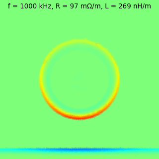
Skin effect in a circular conductor
A copper conductor of 1 mm diameter is subjected to various frequencies of AC excitation. The permeability of both copper and air in this system are taken as approximately \(\mu_0\), which is the vacuum permeability.
Current density is visualized in the cross-section surface with color, but also along the diameter as a 1D plot.


Coaxial cable
A coax of RG316 dimensions
- Inner conductor OD: 0.53 mm
- Inner insulator OD: 1.53 mm
- Outer conductor OD: 1.98 mm
- Outer insulator OD: 2.5 mm
is placed over a ground plane, with center to plane height 1.75 mm. All conductors are made of copper, while \(\mu \approx \mu_0\) for all materials, where \(\mu_0\) is the vacuum permeability.

Consider the two cases:
- Current is balanced between inner and outer conductors: no current flows through the ground plane
- Current flows through the outer conductor and ground plane: no current flows through the inner conductor
Inner - outer


Outer - ground plane


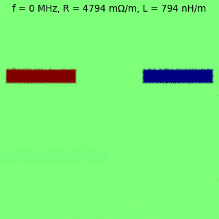
Differential microstrip
Take a differential microstrip of dimensions
- Trace width: 0.2mm
- Trace separation: 0.2mm
- Trace thickness: 0.035mm
- PCB layer thickness: 0.2mm
All conductors are made of copper, with \(\sigma = 5.96\ \mathrm{S} \mathrm{m}^{-1}\) while \(\mu \approx \mu_0\) for all materials, where \(\mu_0\) is the vacuum permeability.

Consider two cases:
- The current enters the left conductor and returns via the right conductor: the odd mode
- The current enters through both the left conductor and the right conductor and returns through the ground plane: the even mode
Odd mode


Even mode


Observations
The higher the frequency, the more concentrated the current and return current are toward each other. With increasing frequency the current is passing through an ever decreasing cross-sectional area. Thus the resistance increases with frequency. On the other hand, the closer the opposite currents are moving to each other, the more the resulting magnetic fields cancel each other out. Thus the inductance decreases with increasing frequency.